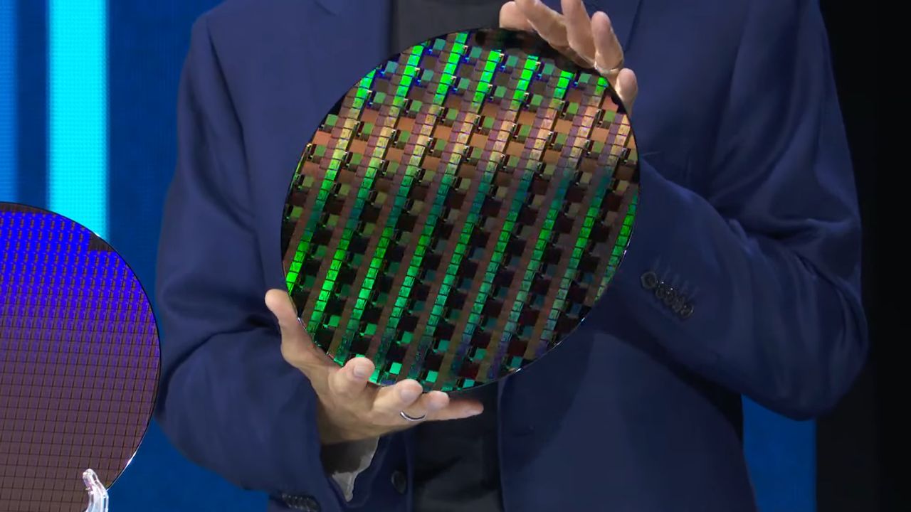
Intel's 18A-P Node: Unpacking the Performance and Efficiency Advances
Intel's next-generation process technology, 18A, is set to receive a significant upgrade with the introduction of the 18A-P variant. This enhanced node promises substantial improvements in performance, power efficiency, thermal management, and manufacturing reliability. Below, we answer the most pressing questions about what 18A-P brings to the table and how it builds upon the already impressive 18A baseline.
What exactly is Intel 18A-P, and how does it differ from the baseline 18A node?
18A-P stands for "18A Performance-enhanced," an optimized version of Intel's 18A process node. While the standard 18A focuses on scaling and density, 18A-P introduces a suite of refinements aimed at pushing clock speeds higher and reducing power consumption. Key differentiators include improved transistor characteristics through optimized gate structures and a redesigned interconnect stack that lowers resistance. These changes result in a claimed 9% performance uplift over baseline 18A at the same power level, or alternatively, a power reduction of similar magnitude at the same frequency. Intel also highlights reduced process variability and better yields, making 18A-P a more mature and reliable choice for high-performance chips.
How much performance improvement can we realistically expect from 18A-P?
According to Intel, 18A-P delivers a 9% performance increase versus the standard 18A node when run at the same power envelope. This is achieved through a combination of higher drive current and lower parasitic capacitance. For example, a processor designed on 18A-P could hit higher turbo clocks without exceeding thermal limits, or run the same frequency at a lower voltage. In real-world workloads like AI inference or gaming, users might see up to a 10% improvement in frame rates or compute throughput, depending on how heavily the application stresses the CPU or GPU. The gain is especially pronounced in scenarios that are sensitive to single-threaded performance or memory latency.
What power efficiency gains does 18A-P offer compared to 18A?
Efficiency is a major focus of 18A-P. By reducing leakage and dynamic power through optimized transistor channel engineering, Intel claims the node can achieve the same performance as 18A while drawing roughly 10-15% less power. This is critical for mobile and data center applications where thermal budgets are tight. For instance, a laptop chip built on 18A-P could extend battery life by an hour or more under typical workloads. Additionally, the improved power delivery network on 18A-P reduces voltage droop, allowing for more aggressive power gating and further efficiency gains in idle states.
How does 18A-P improve thermal conductivity, and why does it matter?
One of the standout features of 18A-P is a 50% improvement in thermal conductivity. Intel achieves this by integrating a new thermal interface material (TIM) and redesigning the backend heat path using thicker metal layers and advanced fin structures. Better thermal conductivity means heat generated by transistors can be dissipated more quickly to the heatsink, resulting in lower operating temperatures. For end users, this translates to higher sustained performance (less thermal throttling) and potentially quieter fans. In dense compute clusters, improved thermals also enhance reliability and allow for tighter packing of chips without overheating.

What are the benefits of reduced process variability and improved yields on 18A-P?
Process variability refers to unintended differences in transistor characteristics across a wafer. 18A-P employs advanced patterning techniques and tighter process controls to minimize these variations. The result is more uniform transistor performance, which reduces the spread between fast and slow chips. This has two key benefits: improved yields (more chips per wafer meet performance targets) and better binning (higher percentage of premium-grade processors). For Intel, this lowers manufacturing costs; for customers, it means greater consistency and fewer defective units. Additionally, reduced variability enables more aggressive overclocking headroom for enthusiasts.
When is 18A-P expected to launch, and which products will use it?
Intel has not announced an official launch date for 18A-P, but based on the 18A roadmap, the enhanced variant is likely to follow roughly 6–12 months after the initial 18A production ramp. Early 18A silicon is expected in late 2024, so 18A-P could arrive in the second half of 2025. The node is expected to be used in high-performance computing (HPC) chips, flagship client processors (such as future Core i9 models), and possibly some data center GPUs. Intel may also offer a version optimised for low-power mobile devices, leveraging the power efficiency gains.
How does 18A-P compare with competing nodes from TSMC and Samsung?
Intel’s 18A-P is positioned to compete directly with TSMC’s N2 (2nm) and N2P processes, as well as Samsung’s 2nm GAA (SF2). While specific benchmarks are not yet public, Intel claims that the 9% performance uplift and 50% better thermal conductivity give 18A-P an edge in peak frequency and thermal management. TSMC’s N2P is expected to offer similar improvements through backside power delivery, but Intel’s unique PowerVia and RibbonFET technologies may provide superior transistor density. In terms of power efficiency, Samsung’s SF2 with GAA could match 18A-P, but yields and variability remain question marks. Overall, 18A-P appears highly competitive, especially for applications that demand both high performance and excellent thermals.
Related Articles
- Critical Kernel Bug: KVM Virtualization Security Feature Triggers Host Hangs
- MINISFORUM Launches Entry-Level M2 Mini PC with Intel Panther Lake; M2 Pro Still Awaiting Release
- 10 Key Takeaways from Dell Technologies World: The Parabolic Rise of Enterprise AI
- SPIFFE Framework Gains Urgency as AI Agents Demand Trustworthy Identities
- Nvidia's Jetson Lineup Faces Early Retirement: DDR4 Memory Shortages Force Accelerated Phase-Out
- 10 Crucial Updates for the nvptx64-nvidia-cuda Target in Rust 1.97
- YouTube Bug Cripples Web Player: Infinite Loop Causes Massive Lag and Memory Drain
- Decoding Strategic Shifts in Tech: A Guide to Understanding Executive Appointments Like Intel's AI Pivot